
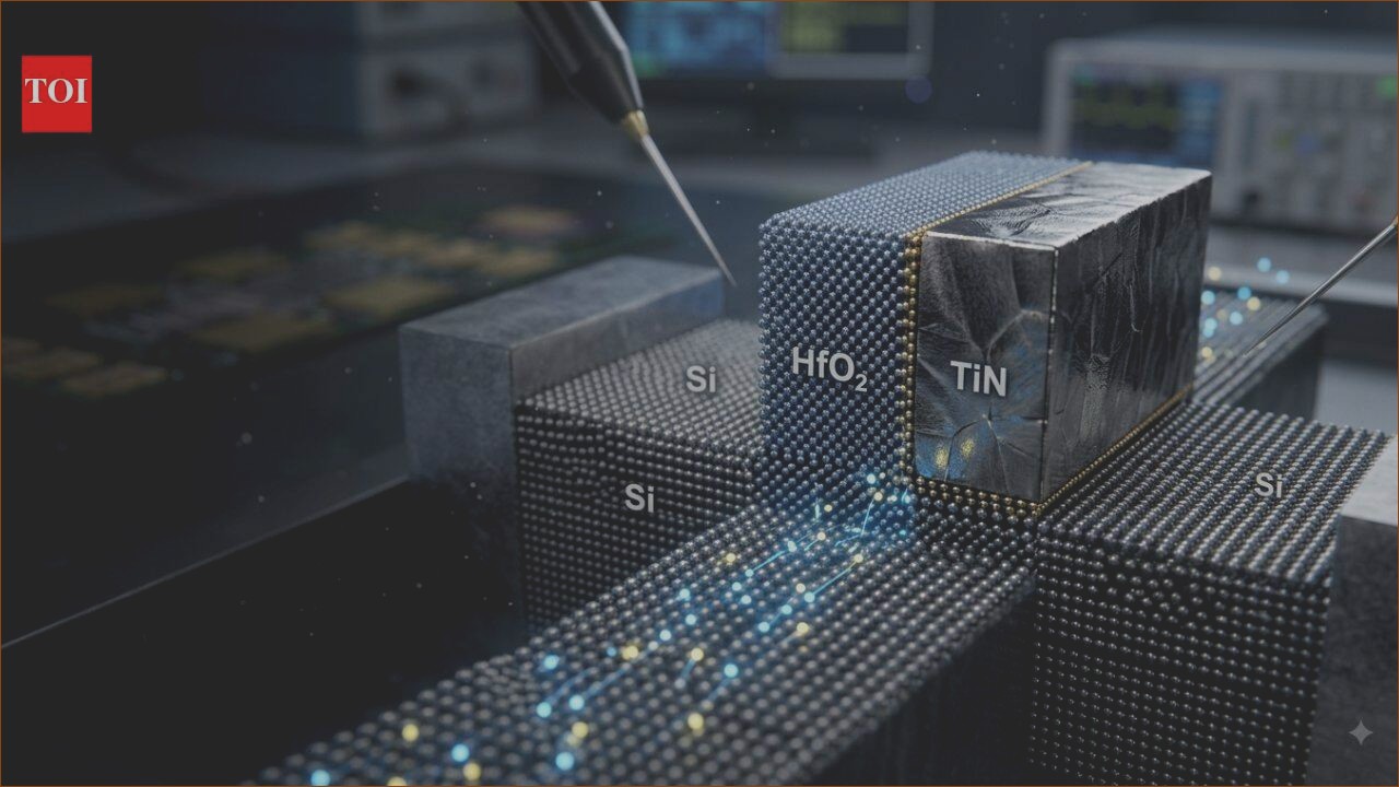
Innovative Approach to Enhance Transistors Using Atomically Thin Materials
Researchers from Taiwan’s National Yang Ming Chiao Tung University (NYCU) and TSMC Corporate Research are making strides in improving transistors crafted from incredibly thin materials. Their focus on the small boundary where two different materials meet has led to the creation of transistors featuring an ultra-thin insulating layer that performs exceptionally well.
What Are Atomically Thin Materials?
For over ten years, scientists have been exploring atomically thin semiconductors. Some of these materials can be just a single atom thick yet still provide useful electrical characteristics. This breakthrough could lead to transistors that are not only smaller and faster but also more energy-efficient than traditional silicon-based devices.
However, achieving consistent performance in these ultra-thin transistors has posed significant challenges. A key issue is the gate dielectric, a tiny insulating layer critical for managing electron movement. While thinning this layer may enhance control over the transistor, it can also lead to complications at the interface with the semiconductor, affecting performance.
Engineering the Atomic Interface
Published in Nature Electronics, the recent study tackles this challenge by refining the atomic interface between the semiconductor and its insulating layer. The NYCU team collaborated with TSMC to improve the connection at this boundary. Instead of simply searching for better semiconductor materials, they focused on optimizing the interface.
Using monolayer molybdenum disulfide (MoS2)—which is composed of just one atom layer—the researchers strategically placed an ultrathin aluminium layer over the MoS2. They then oxidized this aluminium to produce a 0.42-nanometre thick aluminium oxide layer, followed by a layer of hafnium oxide, which provides robust electrical control.
This 0.42-nanometre aluminium oxide layer served as a buffer, smoothing the surface for the hafnium oxide, and minimizing any harmful electrical interactions between the materials.
Significance of the Interface
Transistors made from these atomically thin materials have unique challenges due to their smooth surfaces lacking dangling bonds. This makes it difficult to create a uniform dielectric layer across them. Traditional methods might leave gaps, leading to unwanted defects that can hinder electron movement.
While various dielectric materials and techniques have been tested, achieving a very thin dielectric layer with strong electrical control and high electron mobility has remained challenging. This is particularly critical for monolayer MoS2 produced on a larger scale.
The Role of the 0.42-nanometre Buffer Layer
Rather than replacing the semiconductor or dielectric materials, the researchers redesigned the interface. By placing an ultrathin aluminium layer on the MoS2 and oxidizing it, they created an effective buffer layer. Short-channel top-gate transistors were built using the CVD-grown MoS2, demonstrating low leakage current and minimal hysteresis, enhancing overall performance.
The resulting devices exhibited impressive transconductance, a measure of how well a transistor’s current responds to changes in gate voltage, achieving results that are hard to accomplish with traditional atomically thin transistors.
Looking Ahead: Implications for Future Electronics
These findings underscore the significance of material interfaces as transistors shrink in size. When components are only a few atomic layers thick, the interface plays a critical role in device performance. The ability to engineer these interfaces with precision could open up exciting possibilities for future semiconductor technologies, offering potential advancements that changing individual materials alone cannot provide.
The researchers believe their innovative approach could pave the way for next-generation two-dimensional electronics and bring us closer to practical materials and processes for large-scale manufacturing.
